Recent Advancements in TSMC Packaging Technology
How TSMC Packaging Innovation Fuels the Next Generation of IC Technology
By Ahmed Abu-Hajar, Ph.D.
(October 2025)
Introduction: For much of the past half-century, the relentless miniaturization of transistors fueled an era of rapid progress by designing faster chips with lower power consumption and reduced costs. Yet, without packaging technology advancements, transistor miniaturization alone is not enough to deliver the performance gains demanded by emerging technologies like high-performance computing (HPC) and artificial intelligence (AI). Further gains become increasingly difficult and limited by the packaging parasitic of parasitic effects. This inflecting point has led to look beyond the silicon die itself for new avenues of packaging advancement. IC packaging technologies are now playing a central role in determining the speed, efficiency, and reliability of modern chips. The focus has shifted from merely housing the die for protection to actively include managing signal integrity, power delivery, and heat dissipation.
Modern AI and HPC applications require hardware systems to process massive datasets at unprecedented speeds. The hardware requires enormous parallel processing capabilities and ultra-fast data movement. Advanced IC packaging addresses these needs by enabling multi-die integration in a single package to shorten interconnect distances and to support higher bandwidth. Being able to integrate multi-die in a single package pushed for a paradigm shift in the system design by breaking complex designs into multiple dies (chiplets) that are integrated into a single package. Complex hardware systems are broken into logic, memory, sensors, and analog chiplets which are assembled into a single package, thus creating highly functional and compact system-in-package (SiP). Advanced multi-dies in a single package solution, such as 2.5D and 3D integration, enable high-bandwidth connections between dies, supporting faster data transfer and improved computational throughput. In addition, advanced packaging must reduce power loss and enable finer control over voltage and current to directly impact power efficiency. Therefore, incorporating materials and designs that optimize heat dissipation, allowing chips to operate at higher speeds without overheating.
TSMC as a world leader IC fab has emerged as a pioneer in advanced packaging technology. Recognizing that AI and HPC depend on packaging just as much as on transistor scaling, TSMC has developed several packaging solutions that falls under its 3DFabric® platform. TMSC packaging technology enables system-level scaling and heterogeneous multi-chiplet integration. The platform includes chip-on wafer-on-substrate (CoWoS), integrated fanout (InFo), and system-on-integrated chips (SoIC). These solutions are placed at the heart of AI hardware innovation. In this article we will explain those technologies to engineers and interested readers, but we are first presenting a brief overview of traditional packaging technologies to give the reader an appreciation for the level of advancements in TSMC IC packaging technology. Then we will present an overview of TSMC packaging solution away from depth theoretical and tedious analysis. Interested readers are advised to follow scientific articles in the subject.
Brief Overview of Conventional Packaging Technology: Traditionally, the main purpose of the IC packaging is to provide protection to the fragile die, and to provide connections to external components on the printed circuit board (PCB). The die is encapsulated within a case, and the case protects the die from contamination, corrosion and mechanical damage. Over the years, several packaging styles dominated the industry such as dual inline package (DIP), quad flat package (QFP), ball grid array (BGA) and chip scale package (CSP). The IC package designs involve optimizing electrical performance, mechanical strength, heat dissipation, and electromagnetic interference (EMI). Some packages include heatsinks to allow for spreading heat on the PCB. Conventional packaging has limited input/output (I/O) density, slower signal transmission, higher power consumption, and thermal bottlenecks that prevent chips from scaling to meet modern performance demands.
The structure of conventional IC packages includes an external encapsulating case. The plastic casing is the most popular that is made of epoxy molding compound. Its low cost makes it suitable for commercial production with poor thermal conductivity. Ceramic packages have good insulation, high air tightness and wide range of operating temperature which make them suitable for high-reliability production. Metal casing can be used in hermetic sealed applications, but it is bulky and costly. Internally, Conventional IC packaging is divided into two types: The lead-frame packaging and the substrate-based packaging. The lead-frame packaging provides mechanical support for the chip, and its leads are the pins that electrically connect the internal chip to the external circuits. The chip is placed on a pad at the center of the lead frame, and it is connected to the pins of the lead frame using wire bonds. Also, the lead frame and the package case act as a medium to conduct thermal energy away from the chip. Wire bond is required to connect the die IO pads to the leads (pin) of the chip. Lead-frame technology was initially used in the 1970s for DIPs with 64 pins or less, but various packaging forms have been emerging endlessly. As chip complexity and I/O counts had grown, lead-frame packaging has struggled to keep pace due to interconnect density and routing flexibility. This is where substrate-based packaging took over. Instead of a stamped die on lead-frame, the die is mounted onto a multi-layer organic substrate (often made from epoxy resin with copper wiring), which functions much like a mini printed circuit board. Substrate packaging enables fine-pitch routing, higher signal integrity, and support for advanced features such as flip-chip bonding. In essence, while lead-frame packaging emphasized simplicity and cost, substrate-based packaging unlocked the performance, scalability, and integration.
The substrate-based packaging is mainly divided into two categories, the wire bond substrate-based packaging and the flip chip (FC) substrate-based packaging. The substrate has two sides, the chip side and soldering balls side. The substrate acts as a miniature pcb used to route the signals to their corresponding soldering ball. In the wire bond packaging, the die is mounted on the substrate, while thin gold wires connect the die’s bond pads to the substrate’s metal traces. These wires are typically attached using a thermosonic bonding process where heat, pressure, and ultrasonic energy ensure a reliable electrical connection. The substrate then routes signals and power from the die to solder balls on the bottom of the package, and then it connects to the printed circuit board. To protect the die and delicate bond wires, the package is encapsulated with the epoxy molding compound (or case).
Wire bond substrate-base packaging suffers from higher parasitic inductance, resistance and capacitance due to its longer interconnect lengths compared to an FC substrate-based packaging. FC substrate-based packaging is more suited for high-bandwidth AI and high-performance computing (HPC) processors, to be advanced further by TSMC packaging solution. In the FC structure, the die is mounted face-down on a multi-layer organic substrate, with its active surface, and it is directly interfacing through an array of microscopic solder mini bumps rather than traditional wire bonds. The substrate itself, often made from high-performance materials such as BT resin or Ajinomoto Build-up Film (ABF), contains multiple copper wiring layers that redistribute the dense I/O signals from the die into larger solder balls on the package bottom. These solder balls then connect the package to the printed circuit board. Above the die, an underfill epoxy is applied to strengthen mechanical reliability, distribute stress, and improve thermal cycling endurance. For high-power applications, a heat spreader or heat sink is often attached to the top of the package to manage thermal dissipation. In the following we will present how the FC technology evolved to support TSMC multi-die packaging solutions.
YouTube video that summarizes the history of the IC packing technology ->>
Conventional Packaging Technology

Sample of Lead Frame based IC Package with wire bounding, and encapsulation case. It suffers from extreme RLC parasitic that limits bandwidth, suffers from signal integrity and dissipates heat.

Sample of lead frame with die pad in the center. The lead frame provides mechanical support and electric connection to the external pins.

Sample of wire bond, where a thin gold wire is used to electrically connect the die to the external pins. Wire bond is used in lead frame as well as substrate-based packaging

Example of the soldering ball side and the chip side of the wire bond substrate packaging

FC substrate-based packaging using mini soldering bumps to connect the die to the multilayer substrate. .
TSMC Packaging Technology
In addition to its semiconductor technology, TSMC has emerged as a pioneer in IC packaging technology. Recognizing the complexity of heterogeneous system-level integration with multiple chiplets into single package is as crucial as transistor level advancements. TSMC has developed 3DFabric® platform which is a comprehensive family of 3D die stacking and packaging solutions. The TSMC 3DFabric® provides a holistic packaging design using integrated multi-die systems. It offers 3D silicon stacking and several advanced packaging technologies. Packaging technologies such as Chip on Wafer on Substrate (CoWoS), Integrated Fan-Out (InFO), and System on Integrated Chips (SoIC) are offered to TSMC customers. What sets TSMC apart is not just those unique packaging solutions, but the ability to combine them in a single package. For example, in a multi-chiplet logic-memory system, a CoWoS technology is used for the logic dies, but 3D SoIC is used to stack multi memory dies and then redistributing signals through InFO layers. All are assembled within the same package. This holistic approach enables system architects to design complex systems using system-in-package (SIP) technology.
1. CoWoS Packaging Technology: The CoWoS is TSMC’s 2.5D packaging technology in which it places multiple dies (chiplets) side by side on a large silicon interposer. The interposer is then placed on the substrate which is connected to the external PCB. CoWoS TMSC is divided into three types that are standard (CoWoS-S), redistribution layer (CoWoS-R) and local (CoWoS-L).
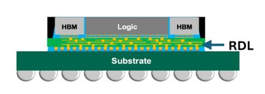
Standard CoWoS-S: In the case of the standard CoWoS-S, the dies are flipped and connected to the interposer using micro-bumps. The micro-bumps are fine scale soldering bumps that connects the die pads to the interposer. The interposer provides ultra-dense and short interconnect wiring, thus allowing for massive bandwidth between dies. This interposer acts as a high-density wiring layer that interconnects the dies with extremely short and fine-pitch signal paths. We may consider the interposer acts as a mini motherboard within the package that connects multi-dies together. The interposer is made of silicon that is fabricated using already matured semiconductor processes to provides micrometer-scale high density metal traces for routing with excellent signal integrity. Through Silicon Via (TSV) is used to connect through the interposer. The entire interposer assembly is then mounted onto an organic substrate using C4 Cu bond-bumps. This allows data to move between the logic die and memory stacks with ultra-high bandwidth and low latency. The substrate provides a distribution to the large power signals and the IO signals from the interposer to the external soldering balls.
Redistribution Layer CoWoS-R: The CoWoS-R has the interposer acts as a redistribution layer (RDL). The RDL serves as interconnect network that links the embedded dies (or chiplets), active logic dies, and high-bandwidth memory (HBM) stacks into a unified electrical system. While the interposer provides mechanical scalability, the RDL determines signal integrity, bandwidth density, and electrical performance. The RDL formation begins after the silicon interposer segments are embedded and the reconstituted wafer surface is planarized to achieve nanometer-scale uniformity. This flatness is essential to ensure tight line width and spacing control across the wafer. The RDL acts as far more than a passive interconnect; it is an active, engineered platform that unites high-density wiring, mechanical reliability, and thermal functionality into one multilayer system.
Electrically, the RDL network handles both high-speed signal routing and robust power delivery. Differential signal pairs and high-speed buses are routed with controlled impedance traces, and TSMC’s design rules specify strict limits on the line width variation, via density, and return path continuity to minimize signal skew and crosstalk.
The fabrication process includes dielectric spin coating, photolithographic patterning, via etching, seed layer sputtering, electroplating of copper, and final passivation. Modern RDL structures achieve line/space dimensions below 2 µm. To maintain such precision over large wafer diameters, advanced stepper lithography or laser direct imaging is used that are coupled with real-time alignment systems to correct die shift during exposure. Copper thickness typically ranges from 2 to 5 µm per layer, optimized for both current-carrying capacity and minimal resistance-capacitance (RC) delay. Multiple RDL layers—often three or more—are stacked vertically, separated by polymer dielectric films and connected through copper-filled microvias.
Localized CoWoS-L: The CoWoS-L bridges the gap between the standard CoWoS-S with a full interposer approach and the redistribution CoWoS-R. CoWoS-L employs a localized RDL instead of a full-sized silicon interposer. The localized RDL is placed where massive interconnect with high bandwidth is needed and lower cost and larger die sizes by. It uses RDL only where fine-pitch routing is essential—directly beneath logic dies and HBM stacks—while delegating coarse-pitch routing to an organic substrate or large build-up RDL layers. Unlike a full CoWoS-S interposer that spans the entire package, the localized approach minimizes silicon area, thereby reducing cost and improving warpage control during assembly. In essence, CoWoS-L represents a strategic synthesis of silicon precision and organic scalability. By localizing high-density interconnect regions only where they are needed.
The thin-film localized RDL layers are formed using advanced photolithographic patterning and electroplated copper metallization, similar to wafer-level BEOL processes. Polyimide or PBO dielectric films are spin-coated between metal layers, providing low-k insulation and mechanical compliance. TSMC addresses this by implementing Through-Bridge Vias (TBVs) or Through-Silicon Vias (TSVs) within the local interposer, combined with copper pillars or micro-bumps that interface to the substrate’s build-up RDL. The transition zone between the local RDL and organic substrate is co-designed with electromagnetic simulation to minimize parasitic inductance and reflection, preserving high-frequency performance up to multi-GHz signaling regimes.
TSMC Through-Silicon Via (TSV) Technology: At the heart of 2.5D/3D system integration lies the Through-Silicon Via (TSV) technology—a vertical interconnect structure that enables signals and power to pass directly through the silicon die. TSVs are the vertical spine of silicon layers to allow vertical interconnects through bulk silicon. TSVs are used in CoWoS-S and SoIC technology, while other variants like (TMVs, TBVs) or hybrid bonding are used in CoWoS-R and CoWoS-L. TSVs allow multiple chips to be stacked with extremely short interconnect paths, reducing latency and power consumption while dramatically improving bandwidth density. This 3D stacking approach contrasts with traditional 2D packaging, where dies communicate laterally through organic substrates. The TSVs, typically filled with copper and surrounded by insulating liners, must be fabricated with nanometer precision to ensure reliability, minimal parasitic capacitance, and mechanical stability. However, challenges such as wafer thinning, via alignment, and thermal stress management remain key engineering bottlenecks.

TSMC packaging technology emerged as a multi-chiplet (or multi-die) integration technology that provides high speed and high bandwidth interconnection among multiple chiplets. The packaging technology emerges as layered 2.5D CoWoS technology, layered InFO packaging or 3D SoIC layered packaging.

The basic structure of CoWoS package. It is made of flipped multi-dies that are placed horizontally side by side on a silicon interposer. The interposer provides routing between the dies. The interposer is placed on a substrate, and the substrate connects to the pcb using soldering balls.

CoWoS package that shows the stack of the chips, interposer and the substrate in a single package. Fine-scale micro bumps are used to connect the dies to the interposer, the interposer to the substrate using C4 Cu bonding bumps. The substrate connects the external signals to the soldering balls.
In the CoWoS-R, the interposer acts as a redistribution layer (RDL) that interconnects multi-dies together and the substrate layer.

CoWoS-L uses local RDL regions for high density routing is used to route signals through the silicon interposer from the micro-bumps to the C4 bumps. Multilayer metals in the RDL may be used for routing.

Through Silicon Via (TSV) is used to route signals through the silicon interposer from the micro-bumps to the C4 bumps. Multilayer metals in the RDL may be used for routing.
2. TSMC InFO Packaging Technology: The integrated fan out chip (InFO) is another TSMC packaging solution as part of the TSMC 3DFabric™. InFO is a wafer-level system integration technology that provides a high-density RDL and Through-InFO Vias (TIVs) for high-density interconnect. InFO offers 2.5D and 3D options optimized for specific applications. The InFO package-on-package (InFO-PoP) is the first 3D wafer-level fan-out package, features a high-density RDL and TIVs. InFO-PoP is mostly used in integrating mobile application processors with DRAM. InFO-PoP has better electrical and thermal performance, and a thinner profile than flip chip package-on-package, because it has no organic substrate or C4 bump. InFO on substrate (InFO-oS) is another version of InFO that leverages InFO technology with higher density redistribution interconnection (RDL).
3. TSMC SoIC Packaging Technology: As HPC and AI systems continue to demand higher bandwidth, power efficiency, and functional density, the semiconductor industry has turned into a 3D packaging innovation. While 2.5D packaging such as TSMC’s CoWoS have revolutionized side-by-side multi-chiplet integration, TSMC SoIC improved the memory-logic integration by stacking multiple active dies vertically, thus forming a true 3D multi-chiplet integration. The TSMC SoIC stacking technology enables die-to-die or wafer-to-wafer bonding with hybrid interconnects. The die-to-die stacks multiple dies vertically, and the wafer-to-wafer stacks the whole wafer vertically. Unlike traditional methods that rely on solder bumps or micro-pillars, SoIC uses direct copper-to-copper (Cu-Cu) bonding combined with dielectric-to-dielectric (oxide-to-oxide) interfaces and thin TSVs. This hybrid bonding approach dramatically shortens interconnect length down to a few micrometers, hence offering extremely low resistance, minimal parasitic capacitance, and unprecedented bandwidth density. The result is near-monolithic performance, where stacked dies behave almost as if they were a single, unified chip.
Structurally, SoIC consists of multiple thinned dies precisely aligned and bonded on top of one another. Each die contains its own active circuitry, power grids, and redistribution layers (RDLs). Once bonded, vertical interconnects are formed by copper vias and hybrid bonds. This creates thousands of high-speed connections between layers. The bottom die, often a high-performance logic processor, is connected to the package substrate through traditional flip-chip or CoWoS interfaces, while upper dies can include additional logic, SRAM, analog, or memory units. This fine-grained vertical integration enables heterogeneous stacking—mixing different process nodes and functions in one compact system.
One key strength of SoIC lies in its integration flexibility. It is designed to work seamlessly with other elements of TSMC’s 3DFabric ecosystem, which includes CoWoS for 2.5D integration and InFO packaging. For example, a high-performance AI chip might use SoIC for vertical logic-memory stacking, mounted on a CoWoS interposer that connects to multiple stacks of HBM, thus combining the strengths of both 2.5D and 3D approaches in one unified architecture. By bringing monolithic-like performance to multi-die systems, SoIC sets the stage for the next evolution in system scaling—beyond the limits of transistor miniaturization. It allows designers to co-integrate compute, memory, analog, and I/O functions with unmatched interconnect density, all within a smaller footprint and lower power envelope.
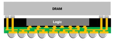
InFO-PoP package where a 3D stack of DRAM is laid over FC on substrate logic chip without the use of interposer. The signals of the top DRAM layer are passed through-InFO Vias (TIVs) to the high density RDL layer.

An example of InFO on Substate (InFO-oS) packaging where 2.5D chiplets are interconnected using a high density RDL and placed on a substrate.

Examples of SoIC packaging that uses 3D die-to-die stacking with homogenous and heterogenous systems. The boding uses fine pitch Cu to Cu connections and thin TSVs to connect the dies vertically.

Wafer-on-wafer 3D packaging technology stacks wafers vertically using tight Cu-CU bonding and thin TSVs to minimize parasitics extremely enhance performance. Once stacked, the bonded wafers are diced into smaller dies. This technology is suited for the same size dies.
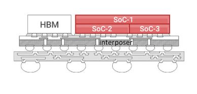
Example of SoIC that supports CoWoS packaging where a 3D homogeneous stack of HBM is integrated with a 3D heterogeneous stack of SoC that are interconnected on an interposer RDL layer.

16 Example of SoIC that supports InFO packaging where a DRAM InFO is integrated over a stack of heterogeneous SoC chiplets.
Roadmap and Competitors: While TSMC stands at the forefront of advanced packaging, the race to define the future of semiconductor integration has become a global competition among the industry’s largest foundries and IDMs. TSMC’s roadmap extends through its 3DFabric platform its proven CoWoS packaging solution toward ever-larger silicon interposers that can support eight or more HBM stacks. In parallel, the company’s SoIC-X initiative is pushing 3D stacking to new limits, enabling denser hybrid-bonded vertical integration for logic-on-logic and logic-on-memory systems.
TSMC is not alone in this race. Intel has made great progress with its Embedded Multi-die Interconnect Bridge (EMIB) technology, which embeds small silicon bridges within an organic substrate to achieve 2.5D integration without requiring a full interposer. Building on this, Intel’s Foveros architecture delivers true 3D stacking by deploying Meteor Lake processors, combining compute, graphics, and I/O tiles into a single compact package. Meanwhile, Samsung’s I-Cube technology is a direct competitor to TSMC’s CoWoS is used on Samsung HBM. Also, Samsung X-Cube 3D stacking solution focuses on logic-memory coupling for AI and HPC. The broader trend is unmistakable: packaging has evolved from a back-end process into a front-line differentiator.
Summary: TSMC has emerged as an advanced IC packaging company in addition to its transistor technology scaling. TSMC 3DFabric™ platform provides multiple 2.5D/3D packaging solutions such as CoWoS, InFO and SoIC. Those technologies allow for multi-chiplets (multi-dies) to be integrated on a single package. CoWoS integrates multiple chiplets over interposer making them act as a single monolithic chip. The SoIC allows for 3D homogeneous/heterogeneous stacking making 3D HBM stacked as a single module and be integrated over 3D heterogeneous SOC chiplets. In this article, we also presented an brief overview of traditional packaging technologies which have led to TSMC packaging technology. The lead frame in traditional packaging suffers for RLC parasitics due to the wire bond and lead frame. This has led to substrate-based packaging which either used wire bond or soldering bumps technologies. TSMC provides multi-chiplet packaging technology, which optimizes performance and costs of complex system integration in a single package.

© 2026-2025 The High-Tech Tribune - All Rights Reserved.