The Evolution of TSMC Transistor Technology for ICs
Continue: The Evolution of TSMC Transistor Technology for ICs
Advantages of GAAFETS
The main advantage of GAAFETs is their superior control of short-channel effects, reduced leakage, and better scalability for advanced nodes. However, they also introduce new fabrication challenges, such as forming uniform nanosheets and precisely wrapping the gate around them at the atomic scale and aggregated capacitances. Despite these hurdles, leading chipmakers like TSMC, Samsung, and Intel are transitioning to GAAFETs to power the next generation of high-performance, low-power chips.
GAAFETs have already moved from research labs into real products. Samsung became the first to mass-produce 3nm GAAFET chips, powering mobile processors and even wearables like the Exynos W1000, where efficiency and compact design are crucial. Other chipmakers, including TSMC and Intel, are preparing to adopt GAAFETs at the 2nm generation for high-performance computing, AI accelerators, and data-center processors that demand maximum density and minimal power loss. With their ability to tame leakage and operate at lower voltages, GAAFETs are also poised to expand into edge devices, IoT, and eventually automotive systems—marking them as the next universal workhorse of advanced electronics.
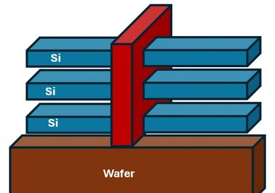
Th Fabrication steps of GAAFETs:
To build multilayer nanosheets, the fabrication process has evolved from the FinFET process. Starting with a silicon wafer, alternating layers of Si and SiGe are grown epitaxially, generating alternating layers of Si/SiGe. The Si layers will form the transistor channels, and the SiGe layers are sacrificial layers and will be etched away later. The Next step is the sheet patterning which defines the areas of the nanosheets. Lithography is used with EUV to define the narrow fins that contain the alternating Si/SiGe. Thin hard mask of SiO2 is deposited to protect the designated layers. Anisotropic etching is implemented by using repetitive steps of reactive ion etching (RIE) process to etch away all the unprotected exposed Si/SiGe layers. The next step is removing the sacrificial SiGe layers by selectively etching them away, leaving behind the suspended silicon nanosheets. The next step is the gate stack deposition to form the gate all around by depositing high-k dielectric around the nanosheets. Then, a metal gate (TiN) is deposited to completely wrap around the nanosheets followed by spacer formation to protect the gate during subsequent steps. The next step is the gate stack deposition to form the gate all around by depositing high-k dielectric around the nanosheets. Then, a metal gate (TiN) is deposited to completely wrap around the nanosheets followed by spacer formation to protect the gate during subsequent steps. The next step is to add contacts to the gates, sources and gates using tungsten, cobalt, or ruthenium, followed by the metallization step where multiple layers of copper are deposited for routing and interconnects.

A stack of Si/SiGe layers added on the top of the substrate (wafer)
Protecting the nanosheets pattern by adding oxide layer using hard mask and lithography.
Etching away the unprotected areas using repetitive steps of anisotropic etching.
Removing the sacrificial SiGe layers, leaving behind the suspended nanosheets.

The gate stack deposited all around the channel for all the layers.
The drain/source heavy doping for n-channel FETs

The drain/source heavy doping for p-channel FETs
Drawback of the GAAFETs
The Gate-All-Around FETs deliver superior electrostatic control but at the price of tougher manufacturing and integration hurdles. The fabrication is far more complex, requiring stacked Si/SiGe layers, precise nanosheet release, and conformal gate deposition. Each has raised costs and risk defects. The ultrathin nanosheets are mechanically fragile, making yield harder to maintain, and material strain adds further reliability concerns. Variability in nanosheet thickness or etch uniformity can shift device performance, while the dense stacking of channels creates power and heat dissipation issues.
Summary
For decades, the planar FET dominated the IC technology, its flat channel and simple one-sided gate design had pushed the rise of microprocessors and consumer electronics. As transistors shrank below 30 nanometers, leakage currents and short-channel effects threatened to stall progress. The shift to FinFET technology, with its three-dimensional fin structure and three-sided gate, has delivered stronger control enabling the explosive growth of smartphones, cloud computing, and AI in the 2010s. Today, as scaling pushes into the 2nm frontier, the industry has embraced the Gate-All-Around FET. By surrounding stacked nanosheets with a gate surrounding the channel from all sides, GAAFETs deliver the ultimate electrostatic control, squeezing out more performance and efficiency. Together, these milestones mark the relentless innovation that keeps Moore’s Law alive.

Table that compares Planar FETs , FinFETs and GAAFETs

© 2026-2025 The High-Tech Tribune - All Rights Reserved.