
PN junction is a diode that passes current in one direction

Two diodes back-to-back are the essential for understanding the evolution FETs. The two back-to-back diodes prevent the current from flowing in both directions.

Applying an electric field from the middle p-type material to the Source (n-type material).

If the electric field is strong enough, it will attract electrons from Source; hence, creating a n-channel from the Drain to the Source. The channel allows the current to flow across the back-to-back diodes.

Applying an electric field from the Source (p-type material) to the middle n-type material.
If the electric field is strong enough, it will repel holes from Source to the middle material; hence, creating a p-channel from the Drain to the Source. The channel allows the current to flow across the back-to-back diodes.
The basic structure of the n-channel FET. A capacitor is created by adding insulator underneath the Gate. The Source and Drain are made of heavily doped n-type material.
When a Gate to Source voltage is applied and the voltage is larger than a threshold value, a n n-channel from the Drain to the Source is created. The Gate to Source voltage creates the electric field required to create the channel.
The basic structure of the p-channel FET, and the Gate is similar to n-channel FET. The Source and Drain are made of heavily doped p-type material.
When a Source to Gate voltage is applied, and the voltage is larger than a threshold value, a p-channel from the Drain to the Source is created.

The current increases once the gate-source voltage increases above the threshold voltage while holding the drain-source voltage constant. Thus, the channel becomes more conductive by increasing the gate-source voltage.

By holding the gate-source voltage constant and increasing the drain-source voltage, the current starts linearly increasing at low values of drain-source voltage, the channel is behaving as a linear resistor. By increasing the voltage, hence the current through the channel increase, the channel gets consumed and it conductivity increases. Eventually the channel gets saturated.
As the transistor size is scaled downward, and the channel length becomes smaller, the effective channel length becomes smaller in the saturation region. This increases the current due to the channel modulation effects at high drain-source voltage.

The gate exhibits large delays during switching because it needs more time to change and discharge gate capacitances. The smaller the transistors, the smaller its capacitances which allows for faster switching.

The fabrication of the n-channel FETs implants heavily doped n-type material on a lightly doped p -type substrate. The gate is developed by adding insulator (SiO2 or high-k material) over the channel region. The insulator is covered by a conductor (e.g. polysilicon) . The substrate is connected to the lowest voltage in the IC via a heavily doped P-type material called Body (B).

When fabricating the FET transistor on ICs, the physical size of the device crucially affects its behavior. The doping concentration, the length of the channel (L), the width of the channel (W) and the thickness of the of the oxide layer (t) directly impacts its behavior.

The p-channel is similar to the n-channel FET, but the substrate is made of n-type material, the drain and source are made of heavily doped p-type material.

IC fabrication mostly uses CMOS technology, in which the n-channel and the p-channel transistors are fabricated on the same wafer. The n-channel is fabricated on the wafer, but the p-channel is fabricated on the n-well. The n-well is implanted on the p-type substrate.

Creating a 3-D FIN Via Etching. The gate surrounds the fin from three sides. The source and the Drain are doped after the
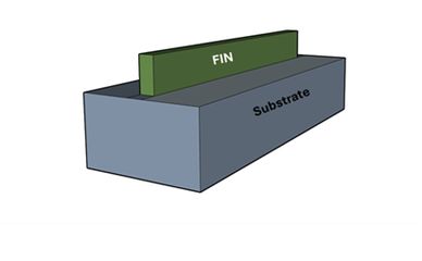
Creating a 3-D FIN Via Etching. The gate surrounds the fin from three sides. The source and the Drain are doped after the

Creating a 3-D FIN Via Etching. The gate surrounds the fin from three sides. The source and the Drain are doped after the

GAAFET is manufactured using lithography process.

GAAFET is manufactured using lithography process.